7408 Logic Gate Chip Ultimate Guide: Pinout, Characteristics and Applications
2025-04-02
12972
In the world of digital electronics, logic gate circuits are the basis for building all complex systems, and IC 7408 is a representative of such basic devices. As a chip integrating four independent dual-input AND gates, IC 7408 is widely used in digital circuit modules such as counters, encoders, and data selectors. This article will systematically and comprehensively introduce the key knowledge points of IC 7408. From its definition, pin function, circuit diagram, to characteristic specifications and working principle, I hope this content can provide you with practical information and technical support.
Catalog
What is IC 7408
The IC 7408, also known as IC 74LS08, is a compact integrated circuit comprising four distinct AND gates, each equipped with dual 8-bit inputs. This IC is a part of the 74XXYY series. AND gates, crucial components of this IC, play a pivotal role in switching logic states. In these gates, two types of logic signals are utilized.
The primary form is a high-level signal, operating within a 3-5V voltage range. Conversely, the secondary form is a low-level signal, akin to a 2-0.2V voltage level. Each AND gate in the 7408 IC requires six input pins and two output pins for proper functioning.
Outputs are capable of existing in both high and low states. However, for the output to be high, both input states must also be high.
Typically, the IC 7408 consists of four AND gates, each capable of operating independently without affecting the others.
Moreover, the 74LS08 needs only a single power source, and its output consistently aligns with TTL devices and other microcontrollers. This makes it a reliable choice for many engineers and electronics enthusiasts.
IC 7408 pinout
The 7408 IC features 14 pins, providing a range of functionalities such as enabling logic gates, and facilitating inputs and outputs.
The pin configuration is as follows
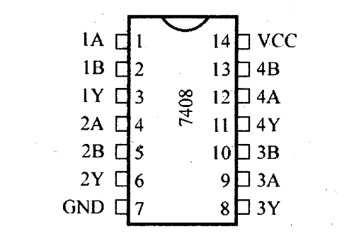
Pin Description
|
Pin |
descriptive |
Pin |
descriptive |
|
1 |
A1-INPUT1 of GATE 1 |
8 |
Y3-Output of GATE 3 |
|
2 |
B1-INPUT2 of GATE 1 |
9 |
A3-INPUT1 of GATE 3 |
|
3 |
Y1-Output of GATE 1 |
10 |
B3-INPUT2 of GATE 3 |
|
4 |
A2-INPUT1 of GATE 2 |
11 |
Y4-Output of GATE 4 |
|
5 |
B2-INPUT2 of GATE 2 |
12 |
A4-INPUT1 of GATE 4 |
|
6 |
Y2-Output of GATE 2 |
13 |
B4-INPUT2 of GATE 4 |
|
7 |
GND - Ground |
14 |
VCC - Positive power
supply |
IC 7408 circuit diagram
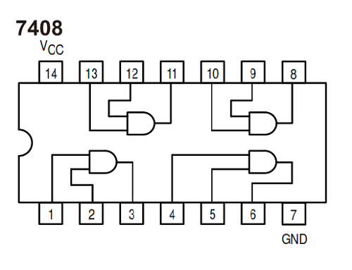
IC 7408 features and specifications
Operating voltage range: +4.75 to +5.25V
Recommended operating voltage: +5V
Maximum supply voltage: 7V
Maximum current allowed through each port output: 8mA
TTL output
Low power consumption
Typical surge time: 18ns
Typical deceleration time: 18ns
Operating temperature: 0°C to 70°C
Storage temperature: -65°C to 150°C
Electronic Specifications
Configuration: Available in SOIC or PDIP packaging, part of the TTL logic series.
14-Pin Dual In-Line (DIL): Provides a standard configuration for ease of use.
Independent 2-Input AND Gates: Comprises four such gates.
Absolute Maximum Ratings: Include a maximum propagation delay of 10 ns, an operating temperature range of -55°C to 125°C, and high-speed operation up to 10 MHz.
Operating Conditions: Power supply voltage (VCC) ranges from 4.75V to 5.25V, with various input and output current and voltage parameters.
- Electrical Characteristics: Detailed specifications of input clamping voltage, high and low-level output voltage, input current, high and low-level input current, short-circuit output current, and supply current.
Equivalents of IC 7408
74LS08: A low-power Schottky version, providing similar functionalities but with typically lower power consumption and slightly different electrical characteristics.
74HC08: A high-speed CMOS version, renowned for operating at higher speeds compared to the standard TTL version.
74HCT08: A high-speed CMOS version compatible with TTL, combining the advantages of CMOS technology with compatibility to TTL voltage levels.
Working Principle of IC 7408
The IC 7408 contains four AND gates, each receiving two input signals. Each gate performs the basic AND operation, meaning if both inputs are high (logic level 1), the output is high (1). If any input is low (logic 0), the output is low. Based on the principles of TTL (Transistor-Transistor Logic), the IC 7408 generates outputs for each gate, which are transmitted through the respective output pins. Hence, the IC 7408, known for its four 2-input AND gates, is widely used in various electronic applications due to its versatility and reliability.
How to use IC 7408
The IC 7408 employs AND gate logic, which comes in three types of combinations. Each combination generates an output level based on a specific input operation level. In this case, the AND gates are implemented using transistors.
As illustrated in the diagram below
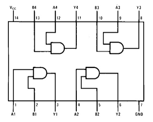
The chip contains four DNA ports internally connected, with each AND port performing an AND operation on two logical inputs. For example, port 1 carries out a DNA operation between A1 and B1, providing output at terminal Y1.
The truth table for the AND gate is as follows
|
Input1 |
Input2 |
Input3 |
|
LOW |
LOW |
LOW |
|
HIGH |
LOW |
LOW |
|
LOW |
HIGH |
LOW |
|
HIGH |
HIGH |
HIGH |
To exemplify the above concept, let's consider a simple application circuit of an AND gate, as shown in the next diagram.
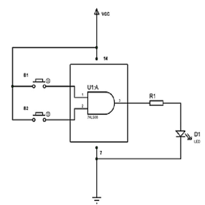
For a better understanding of the internal workings, we can refer to the simple internal circuit of an AND gate, depicted below.
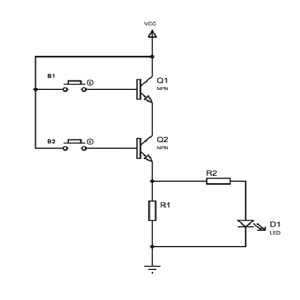
In this circuit, two series transistors form an AND gate. The two input terminals of the AND gate stem from the base terminals of these two transistors. These inputs connect to nodes to alter the logic of the inputs. The output of the AND gate is the voltage across resistor R1. This output is linked to LED D2 through a current-limiting resistor R1 to detect the output state.
The active circuit can be divided into the following stages
Stage 1: When neither button is pressed, the current at the dry ends of both transistors is zero. Consequently, transistors Q1 and Q2 are OFF, causing the total VCC power voltage to appear across them. Since the total VCC appears across the transistors, there is no voltage drop across resistor R1, resulting in a low-level output. Thus, when the input is low, the output is low.
Stage 2: When any button is pressed, one transistor opens, and the other closes. The ON transistor acts as a short circuit, while the OFF transistor acts as an open circuit, displaying the total VCC. At this point, the voltage drop across resistor R1 is zero, maintaining the output at a low level. Therefore, when the input is low, the output remains low.
Stage 3: When both buttons are pressed, both transistors conduct, and the voltage across them is zero, causing the total VCC to appear across resistor R1. Since the output is merely the voltage across resistor R1, it is high. Hence, when both inputs are high, the output is high.
After verifying these three states, it's evident they satisfy the truth table mentioned above. Additionally, the logic equation of the AND gate can be written using the truth table, i.e., Y = AB or A + B. Therefore, each port of the chip can be utilized as needed.
Furthermore, it's important to note that a single AND gate or a combination of 2 AND ports cannot create different logic gates. However, AND gates can be used to fabricate other logic gates. For instance, an AND gate can be transformed into a NAND gate using an N0 gate. AND gates play a crucial role in designing other logic gates like XNOR and XOR. But, if an AND gate is combined with another logic gate, it can create a new logic gate, such as combining NOT, OR, etc.
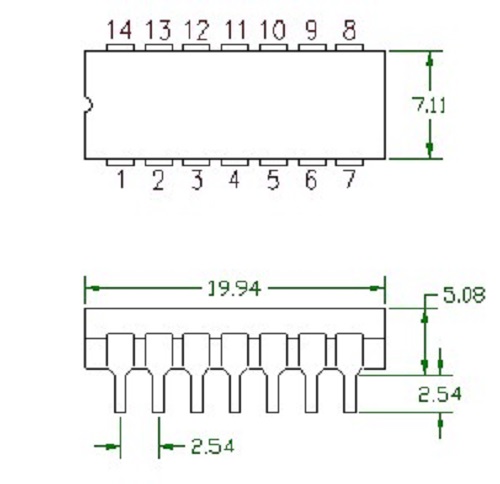
Size of IC 7408
Where the IC 7408 is used
The 7408 IC, also referred to as IC 74LS08, has a wide array of applications. It is particularly used in scenarios that require AND logic operations. The chip contains four DNA ports, and it is possible to use one or all of these ports simultaneously.
The chip is employed in systems that need high-speed DNA operations. As previously mentioned, the ports within the chip are designed using Schottky diodes to reduce the delay in switching the ports. Hence, the chip is well-suited for high-speed AND operations.
Furthermore, this chip provides the TTL outputs required by certain systems.
Applications of the IC 7408 include
Digital Logic Gates
Binary Counters
Multiplexers
Flip-Flops
Bus Drivers/Receivers
Address Decoders
Data Latches
Logic Gate Circuits
Decoders
Shift Registers
Counters
Arithmetic Circuits
In conclusion
The 7408 chip is extensively utilized in digital circuit design and logic control circuits. It performs the logic AND function, delivering a high output only when all input signals are high, a crucial aspect in digital circuits. Moreover, cascading multiple 7408 chips allows for the realization of more complex logic functions.
However, when using the 7408 chip, certain considerations are necessary:
The input signal's voltage range must be within the range specified in the chip's datasheet. Exceeding this range might lead to malfunctioning or damage to the chip.
The loading capacity of the input signal should be considered. If it needs to be connected to other circuits or logic gates, ensure stable signal transmission.
The timing relationship of input signals also needs consideration. In some designs, input signals may have a sequence in time, which should be connected reasonably according to design requirements.
Summarizing, the 7408 chip is a basic logic gate chip featuring four AND gates. It is widely applied in digital circuit design and logic control circuits. Attention should be paid to the input signal's voltage range, loading capacity, and timing relationship.
 ABOUT US
Customer satisfaction every time. Mutual trust and common interests.
function test. The highest cost-effective products and the best service is our eternal commitment.
Hot Article
- Are CR2032 and CR2016 Interchangeable
- MOSFET: Definition, Working Principle and Selection
- Relay Installation and Testing, Interpretation of Relay Wiring Diagrams
- CR2016 vs. CR2032 What’s the difference
- NPN vs. PNP: What's the Difference?
- esp32 vs stm32: which microcontroller is better for you?
- LM358 Dual Operational Amplifier Comprehensive Guide: Pinouts, Circuit Diagrams, Equivalents, Useful Examples
- CR2032 VS DL2032 VS CR2025 Comparison Guide
- Understanding the Differences ESP32 and ESP32-S3 Technical and Performance Analysis
- Detailed Analysis of RC Series Circuit
 LR44 vs 357: Is LR44 Same As 357
2023-12-05
 The Ultimate Guide to LM317 Transformers: Data, Characteristics, and Their Applications
2023-12-01
Frequently Asked Questions [FAQ]
Frequently Asked Questions [FAQ]
1. What is the name of the IC 7408?
The 7408 IC is a two-input NAND gate, also known as a hex inverter. It comprises six such inverters, each capable of independent use. On any of these inverters, if the input is low, the output is high, and vice versa.
2. Why do IC numbers start with 74?
The number 74 identifies the IC as a commercial-grade member of the series. These devices are typically packaged in plastic 14-pin, 16-pin, or 24-pin Dual In-line Packages (DIP) and operate under a power supply range of +4.75 V to +5.25 V, in a temperature range of 0°C to +70°C.
3. What are some real-world examples of logic gates?
The application of logic gates depends mainly on their truth tables, i.e., their mode of operation. Basic logic gates are used in many circuits, such as button locks, light-activated burglar alarms, safety thermostats, automatic watering systems, etc.
4. How many gates does a CPU have?
Logic circuits include devices like multiplexers, registers, Arithmetic Logic Units (ALU), and computer memory, up to complete microprocessors, which might contain over a hundred million logic gates.
Hot Part Number
 GRM188R72A392KA01D
 EMK316B7225KLHT
 GRM0335C1H3R2BD01D
 TPSD685M035R0400
 CMJ206T32768DZFT
 VS-42CTQ030STRLPBF
 BA4510FV-E2
 CY7C2670KV18-450BZI
 BD6962FVM-TR
 ATMEGA88V-15AT
- HI9P0201-5Z
- AL8861Y-13
- IRMCF143TR
- 6R1MBI75P-160-54
- 7MBR30UA060
- TPSX475M050R0500V
- XC9572XL-10TQ100C
- SN74LVC2G32DCTR
- AD2S90APZ
- T491D476M010AH
- ADV7201LST2
- AT73C501-JI
- BSC072N03LDG
- GCIXF6012EE.B1
- LAN91C113I-NC
- LPC47M287-NR
- MT5362ANG
- PI3B16861AX
- PI49FCT3807QEB
- PT4115B89E
- SI2433-KT
- SN0307061
- TP2858HQN
- UPC272G2-T1
- BA4116FV-E1
- CF77496A
- CGY2013AHL/C1
- CS8553GG
- M6117C-A1
- TXC-05870AIBG
- AN2121SC
- KA5Q0765RTHYDT
- MMSZ5231B-V-GS08
- TM512AC4
- K5L5628ATB-DF66
- S12311PRI
- CXP82432A-190Q
- 15WB60
- ROS-2750+