ASIC vs FPGA: Which One Should You Choose?
2026-04-24
281
Catalog
Understanding ASIC and FPGA Basics
An Application-Specific Integrated Circuit (ASIC) is a custom-designed chip created to perform a specific function. Unlike general-purpose processors, an ASIC is built for a single application, allowing it to achieve high speed and low power consumption. ASICs are fixed after manufacturing, meaning their functionality cannot be changed, which enables optimized performance for a defined task.
A Field-Programmable Gate Array (FPGA) is a programmable chip that can be configured after manufacturing. Unlike ASICs, an FPGA allows hardware functionality to be modified as needed, making it suitable for systems that may require updates or design changes over time.
How ASIC and FPGA Function
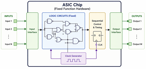
Figure 2. How an ASIC Processes Signals Using Fixed Hardware Logic
How ASICs Work
ASICs execute a fixed function directly in hardware. Input signals are processed through dedicated logic circuits designed for a specific task. Sequential control manages timing, and the system produces the required output.
Since the function is built into the hardware, ASICs achieve high speed and efficient operation.
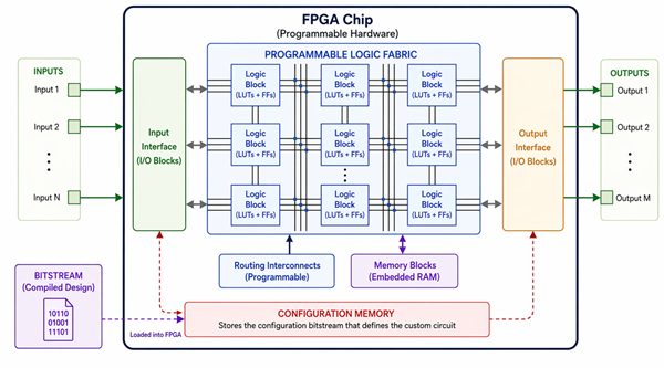
Figure 3. How an FPGA Processes Signals using Programmable Logic
How FPGAs Work
FPGAs use programmable hardware to create custom circuits. They include logic blocks, routing interconnects, memory, and input/output interfaces.
Designs are written using hardware description languages and loaded as a bitstream, allowing the device to be reprogrammed when needed.
Core Architectural Differences
ASIC Architecture
• Custom transistor-level design - Provides precise control over hardware for optimized performance.
• Optimized for specific tasks - Focused design improves speed and reduces excess complexity.
• High efficiency - Only required components are implemented, minimizing power and area usage.
FPGA Architecture
• Programmable logic blocks - Enable circuit creation and modification after manufacturing.
• Reconfigurable routing - Allows connections to be adjusted for different designs.
• High adaptability - Hardware can be updated without creating a new chip.
ASIC and FPGA Development Process
ASIC Development Steps
1. System Specification: Defines functionality, power budget, and performance targets. Incomplete specifications often lead to costly redesigns later.
2. Architecture and RTL Design: Implements logic using HDL. Trade-offs between area, speed, and power are decided at this stage.
3. Verification: Covers simulation and testbench validation. Most project delays occur here due to corner-case bugs.
4. Synthesis and Optimization: Transforms RTL into gate-level design. Timing closure and area constraints become critical.
5. Design for Testability (DFT): Adds scan chains and test logic. Poor DFT design increases production test cost.
6. Physical Design: Includes placement and routing. Congestion and timing violations are common challenges.
7. Tape-Out: Final design sent for fabrication. Errors at this stage are extremely expensive.
8. Fabrication and Packaging: Wafer manufacturing and chip packaging. Yield and defect rate affect final cost.
9. Testing and Validation: Post-silicon validation. Real hardware issues often differ from simulation results.
FPGA Development Steps
1. System Specification: Defines logic functions, interface requirements, clock targets, and resource limits. Poor early planning often causes timing or pin assignment changes later.
2. Design Entry (HDL): Describes hardware behavior using Verilog, VHDL, or block-based design tools. Clear module boundaries make simulation and debugging easier.
3. Simulation and Verification: Tests the design before hardware implementation. Many FPGA issues come from missed edge cases, reset behavior, or clock-domain crossing errors.
4. Synthesis: Converts HDL into FPGA logic resources such as LUTs, flip-flops, RAM blocks, and DSP blocks. Resource usage becomes visible at this stage..
5. Constraints and Timing Setup: Defines clocks, input/output delays, pin assignments, and timing limits. Incorrect constraints can make a design look correct but fail on real hardware.
6. Place and Route: Maps the synthesized design into physical FPGA resources. High utilization may cause routing congestion and timing violations.
7. Timing Analysis: Checks whether signal paths meet setup and hold requirements. Failed timing often requires logic optimization, pipelining, or clock strategy changes.
8. Bitstream Generation: Creates the configuration file loaded into the FPGA. This step depends on successful implementation and valid design constraints.
9. Hardware Testing: Validates the design on the target board. Real-world testing often reveals signal integrity, power, reset, or interface issues not seen in simulation.
Different Types of ASIC and FPGA
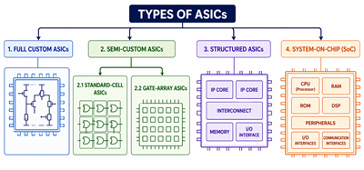
Figure 4. Types of ASICs and their Classifications
Types of ASICs
Full Custom ASICs: Designed at the transistor level for maximum performance.
Semi-Custom ASICs: Built using IP cores for faster development.
• Standard-cell ASICs
• Gate-array ASICs
Structured ASICs: Use predefined frameworks to simplify design.
System-on-Chip (SoC): Integrate processors, memory, and interfaces into one chip.
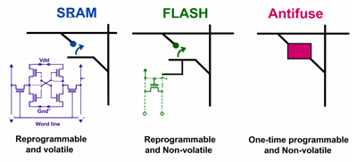
Figure 5. Types of FPGAs based on Configuration Technology
Types of FPGAs
SRAM-Based FPGAs: Volatile and widely used.
Flash-Based FPGAs: Non-volatile with lower power use.
Antifuse FPGAs: One-time programmable and highly secure.
Applications of ASICs and FPGAs
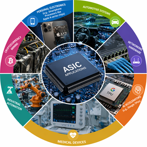
Figure 6. ASIC Applications Across Major Industries
ASIC Applications
• Personal electronics (e.g., smartphone processors like Apple A-series chips)
• Automotive systems
• Networking hardware
• AI accelerators (e.g., Google TPUs)
• Medical devices
• Industrial automation
• Cryptocurrency mining
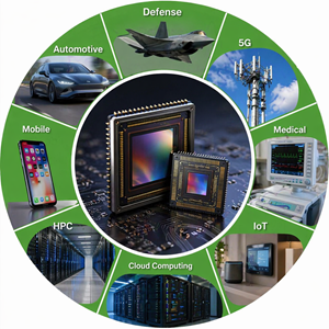
Figure 7. FPGA Applications in Modern Technology
FPGA Applications
• Telecommunications (e.g., 5G base stations)
• Automotive systems
• Aerospace and defense
• Industrial automation
• Medical devices
• AI and data centers
• Prototyping and research
ASIC vs FPGA Comparison
|
Feature |
ASIC |
FPGA |
|
Function |
Fixed |
Reprogrammable |
|
Performance |
High |
Moderate to high |
|
Power Efficiency |
High |
Lower |
|
Upfront Cost |
High |
Low |
|
Unit Cost |
Low at scale |
Higher |
|
Flexibility |
Limited |
High |
|
Time-to-Market |
Longer |
Faster |
How to Choose Between ASIC and FPGA
Use an FPGA when requirements may change, fast hardware validation is needed, or expected volume is low. FPGA avoids mask and fabrication NRE, making it practical for prototypes, test systems, industrial equipment, and low-volume products.
Use an ASIC when the design is stable, shipment volume is high, and lower unit cost or better power efficiency matters more than flexibility. ASIC projects require high upfront NRE for design, verification, masks, IP, packaging, and validation.
A practical suggestion: choose FPGA for early validation or thousands of units; choose ASIC when volume reaches hundreds of thousands or millions of units and the lower chip cost can offset upfront development cost.
|
Decision
Factor |
FPGA
Is Better When |
ASIC
Is Better When |
|
Production
volume |
Tens
to thousands of units |
Hundreds
of thousands to millions of units |
|
Upfront
cost |
Low
NRE or no mask cost needed |
High
NRE can be recovered over volume |
|
Development
time |
Fast
prototype or market entry needed |
Longer
design and fabrication cycle is acceptable |
|
Design
flexibility |
Requirements
may change after launch |
Function
is fixed and stable |
|
Unit
cost |
Higher
unit price is acceptable |
Lower
cost per chip is needed at scale |
|
Power
efficiency |
Moderate
power is acceptable |
Power
and thermal limits are strict |
|
Performance |
Good
enough with programmable logic |
Optimized
silicon performance required |
Conclusion
ASICs and FPGAs serve different purposes depending on performance, cost, and flexibility needs. ASICs are ideal for stable, high-volume designs, while FPGAs are better for adaptable and faster development projects. Understanding their differences helps in choosing the right solution for efficient system design.
function test. The highest cost-effective products and the best service is our eternal commitment.
Hot Article
- LM358 Dual Operational Amplifier Comprehensive Guide: Pinouts, Circuit Diagrams, Equivalents, Useful Examples
- Are CR2032 and CR2016 Interchangeable?
- Understanding the Differences ESP32 and ESP32-S3 Technical and Performance Analysis
- Choosing the Right Battery: A Guide to AG4, LR626, LR66, 177/376/377, SR626, and SR626SW Equivalents
- NPN vs. PNP: What's the Difference?
- BC547 Transistor Basics: Pinout, Application Circuits, Alternative/Complementary Models
- esp32 vs stm32: which microcontroller is better for you?
- What Is a MOSFET and How It Works?
- Electrical Relay Basic: Working Operation, Types and Uses
- PNP Transistors: Structure, Working Principle and Application
 How to Improve Signal with High Pass Filters
2026-04-24
 Binary Decoders Explained: Types, Functions and Applications
2026-04-23
Frequently Asked Questions [FAQ]
1. Do ASICs or FPGAs consume more power?
ASICs generally consume less power because they are optimized for a specific function, while FPGAs use more power due to their flexible design.
2. Can ASIC designs be modified after manufacturing?
No, ASICs cannot be changed once manufactured, which is why careful design and testing are important.
3. Can an FPGA replace an ASIC in production systems?
Yes, but only for low to medium production volumes. ASICs are still better for large-scale production due to lower cost per unit.
4. Why are ASICs more expensive to develop?
ASICs require custom design, fabrication, and testing, which involves high upfront costs and specialized tools.
5. How long does it take to develop an ASIC vs FPGA?
ASIC development can take months to years, while FPGA development can be completed much faster since no fabrication is needed.
6. Are FPGAs used in artificial intelligence applications?
Yes, FPGAs are used in AI for tasks that need flexibility, fast updates, and high-speed data processing.
7. What programming languages are used for FPGA design?
FPGAs are typically designed using hardware description languages like Verilog and VHDL.
Hot Part Number
 C0402X6S0G331K020BC
 GRT31CR61E475KE01L
 GR442QR73D221KW01L
 GRM0335C1E2R7CA01J
- GRM033R71E332KA12J
 EMK063B7682KP-F
 CS1206KKX7RYBB473
 LD02YC181KAB2A
 12105C154KHT1A
 1812GA221JAT9A
- T495X336M025AHE200
- DSI30-12A
- SI6975DQ-T1-E3
- SL38160AZC-18AHT
- MAX3232EEUE+T
- MT48LC4M16A2P-6:G
- MAX6356TWUT+T
- LCMXO1200C-5FTN256C
- FP15R12KT3
- LTC3638IMSE#PBF
- T491A474M025AT7622
- TMS320C6455BCTZ7
- T491D106K035AH2478
- T491X226M035ATAUTO
- T491C475M035ZTAU00
- ST7FLITE02Y0M6
- LT4256-1IS8#PBF
- LM2594MX-5.0/NOPB
- GE212JIYJ23JB
- GE28F256L18B
- HD64F2329BVTE25
- ICS93722CF
- IS61LPS51236A-200TQL
- KSZ8841PMQL
- MT41K256M16TW-107IT:P
- MT49H16M18CFM-5IT
- P51XAG37KBBD
- ST19NP18ER28PVMX
- STPR1020CTW
- AK4311AVM-E2
- LR36A11A
- NAT7210BPD
- IH5047MJE/883B
- MAX232MJE/883
- MM3Z2V4S
- GS8662Q18BGD-300
- AD8876ACPZ
- WL2851E33-5/TR
- BM05B-PASS-TF