PCF8574T I/O Expander Guide
2024-10-09
1460
Catalog
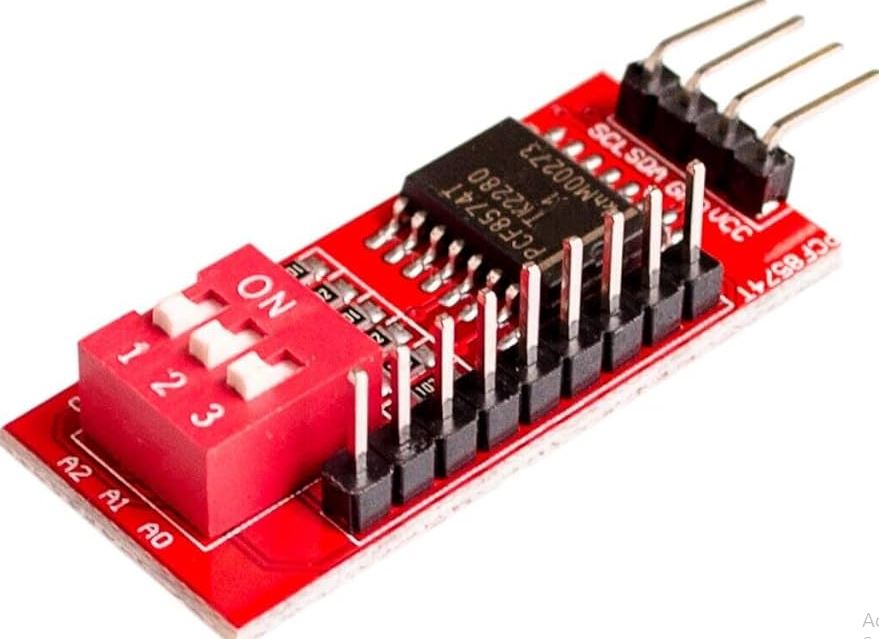
PCF8574T I/O Expansion Board
The PCF8574T I/O Expansion Board operates as an 8-bit I/O expander specifically designed for the I2C-bus. This configuration allows up to 8 expansion boards to connect to a single I2C-bus, collectively managing up to 64 I/O ports. The board's setup streamlines multiple module connections through pin headers and connectors. Additionally, an onboard potentiometer allows for precise adjustments to the LCD backlight, while a jumper cap oversees the LED switch for efficient energy management.This I/O expansion board demonstrates its versatility in various applications, including embedded systems and dynamic electronic projects where the enhancement of I/O ports brings substantial benefit.
You have lauded its seamless modularity, which simplifies the expansion process. This modular design proves invaluable in projects where scaling I/O ports is required without adding undue complexity to the system's overall design. The onboard potentiometer is appreciated for its role in adjusting the LCD backlight. This functionality provides with a method to fine-tune their displays, enhancing readability under fluctuating lighting conditions.
The PCF8574T I/O Expansion Board enhances I/O capabilities across diverse electronic projects. Its modular design, complemented by features such as the LCD backlight adjustment and LED switch control, offers considerable flexibility and oversight. Its capacity to scale, applications, and expert advice illustrate its role in supporting complex and expandable electronic systems.
PCF8574T CAD Models
The PCF8574T microcontroller enhances its utility by offering multiple CAD models. Specifically, these include Symbol, Footprint, and 3D Models. These elements contribute to smoother design processes by enabling integration into sophisticated design software, ultimately aiding effective prototyping and development.
Symbol Models

Symbol models provide a graphical representation of the PCF8574T in schematic diagrams. You find that predefined symbol models can markedly shorten design time, allowing a sharper focus on the functional and performance qualities of prototypes.
Footprint Models
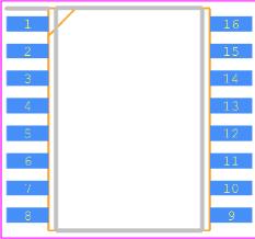
Footprint models offer precise physical layout patterns for the PCF8574T in PCB design. These models ensure correct placement and connection points for smooth signal flow and device stability. In practice, accurate footprint models can prevent costly manufacturing mistakes, thereby optimizing resource allocation.
3D Models
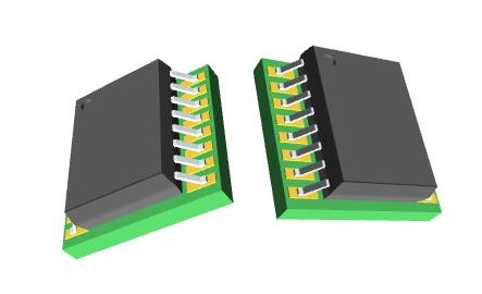
3D Models provide a tangible visualization of the PCF8574T within a virtual 3D environment. This feature allows multi-angle inspection and compatibility checks with various mechanical components.
PCF8574T Pinout and Configuration
The PCF8574T acts as an interface bridge for the I²C-bus, connecting the microcontroller to less complex peripheral circuits. This powerful device features an 8-bit quasi-bidirectional I/O port (P0-P7), an I²C-bus interface (SCL and SDA), and essential power supply pins (VCC and GND).
|
Pin No |
Pin Name |
Description |
|
1 |
A0 |
address input 0 |
|
2 |
A1 |
address input 1 |
|
3 |
A2 |
address input 2 |
|
4 |
P0 |
quasi-bidirectional I/O 0 |
|
5 |
P1 |
quasi-bidirectional I/O 1 |
|
6 |
P2 |
quasi-bidirectional I/O 2 |
|
7 |
P3 |
quasi-bidirectional I/O 3 |
|
8 |
VSS |
supply ground |
|
9 |
P4 |
quasi-bidirectional I/O 4 |
|
10 |
P5 |
quasi-bidirectional I/O 5 |
|
11 |
P6 |
quasi-bidirectional I/O 6 |
|
12 |
P7 |
quasi-bidirectional I/O 7 |
|
13 |
INT |
interrupt output (active LOW) |
|
14 |
SCL |
serial clock line |
|
15 |
SDA |
serial data line |
|
16 |
VDD |
supply voltage |
Power and Ground Connections
Pin VCC supplies power to the IC and should be connected to a stable supply voltage from 2.5V to 6V. Pin GND serves as the ground return for the IC and ought to be connected to the system ground. In this applications, ensuring a stable and noise-free power supply for reliable performance. Power disturbances often result in erratic behavior in connected peripherals, a realization often experienced in troubleshooting phases.
I²C-bus Interface Pins
The SCL (Serial Clock) and SDA (Serial Data) pins function as the communication conduit between the microcontroller and the PCF8574T. Appropriate pull-up resistors on these pins are required. Such resistors prevent communication errors and maintain signal integrity, a common and trusted practice in I²C bus systems.
I/O Port Pins (P0-P7)
Pins P0 to P7 make up the 8-bit quasi-bidirectional I/O port which can be individually configured as input or output. These versatile pins can control LEDs, relays, or read sensor states. Each port pin comes with a weak internal pull-up resistor. When set as input, the pin can directly connect to peripheral devices. Thoughtful configuration of these pins can reduce both software complexity and hardware costs, enhancing design efficiency.
Address Pins Configuration
With three address pins (A0, A1, and A2), the PCF8574T allows up to eight devices to connect on the same I²C bus, avoiding address conflicts. Proper assignment and wiring of these pins ensure multiple devices coexist seamlessly. This feature brings flexibility and scalability into system design.
I/O Port Characteristics
The quasi-bidirectional nature of the I/O ports means they can source current when set high and sink current when set low. This characteristic simplifies interfacing, reducing the need for external components. Designing with these ports, programmers often discover that correct port configuration can prevent unintended signal conflicts, streamlining both the design and testing phases.
Specifications
|
Type |
Parameter |
|
Factory Lead Time |
7 Weeks |
|
Package / Case |
16-SOIC (0.295, 7.50mm Width) |
|
Number of I/Os |
8 |
|
Packaging |
Tube |
|
JESD-609 Code |
e4 |
|
Moisture Sensitivity Level (MSL) |
2 (1 Year) |
|
Terminal Finish |
Nickel/Palladium/Gold (NiPd/Au) |
|
Terminal Position |
DUAL |
|
Peak Reflow Temperature (Cel) |
260 |
|
Terminal Pitch |
1.27mm |
|
Base Part Number |
PCF8574 |
|
JESD-30 Code |
R-PDSO-G16 |
|
Output Type |
Push-Pull |
|
Interface |
I2C |
|
Number of Bits |
8 |
|
Supply Current-Max |
0.1mA |
|
Interrupt Output |
Yes |
|
Features |
POR |
|
Height Seated (Max) |
2.86mm |
|
RoHS Status |
ROHS Compliant |
|
Mounting Type |
Surface Mount |
|
Surface Mount |
YES |
|
Operating Temperature |
-40°C~85°C |
|
Published |
1997 |
|
Part Status |
Active |
|
Number of Terminations |
16 |
|
Voltage - Supply |
2.5V~8V |
|
Terminal Form |
GULL WING |
|
Supply Voltage |
5V |
|
Time@Peak Reflow Temp-Max (s) |
NOT SPECIFIED |
|
Pin Count |
16 |
|
Qualification Status |
Not Qualified |
|
Power Supplies |
3/5V |
|
Number of Ports |
1 |
|
Clock Frequency |
100kHz |
|
External Data Bus Width |
1 |
|
Current - Output Source/Sink |
300μA 25mA |
|
Length |
10.3mm |
|
Width |
7.5mm |
NXP's PCF8574T/3,512 is notable for its detailed technical specifications and adaptable parameters, integrating well with similar components. Several distinctive features contribute to its versatility across various applications.
Electrical Characteristics
Operating within a voltage range of 2.5V to 6.0V, the PCF8574T/3,512 adjusts smoothly to diverse power environments. This adaptability permits straightforward system integration with minimal alterations. Its low standby current consumption renders it highly suitable for battery-operated devices. The input and output current characteristics endorse robust performance and reliable operation under different load conditions. Additionally, the device’s electrical resilience provides extra protection in complex circuits, enhancing both durability and reliability.
Interface and Communication Features
The PCF8574T/3,512 is equipped with an I2C interface that ensures seamless communication with microcontrollers and other digital systems. The I2C bus, by diminishing wiring complexity and offering solid error handling, makes integration smoother and more reliable. These observations indicate that the I2C’s versatility enables to manage multiple peripherals using just two communication lines, optimizing space and resources in tight environments.
Operational Performance
The PCF8574T/3,512 enhances the I/O capacity of microcontrollers, expanding the system’s ability to interface with additional sensors or actuators without requiring more microcontroller pins. The device’s fast response times ensure efficient real-time data processing and management for applications necessitating high-speed communication and control.
Features of PCF8574T
The PCF8574T showcases a blend of versatile features that enhance its utility in diverse applications. These include its role as an I2C to parallel port expander, its reliable 100 kHz standard-mode I2C-bus interface, and an adaptable operating voltage range spanning 2.5V to 6V. Below are comprehensive details on these features:
I2C to Parallel Port Expander
The PCF8574T operates effectively as an I2C to parallel port expander, extending I/O capabilities and streamlining complex circuit designs. Utilizing this functionality can achieve maximum resource efficiency in their designs, reducing the need for a multitude of additional components.
I2C-Bus Interface
Conducting operations at a 100 kHz standard mode, the I2C-bus interface of the PCF8574T ensures smooth communication between the master and multiple slave devices. This facilitates seamless integration into diverse applications, such as home automation systems and industrial control units.
Operating Voltage Range
The device supports a versatile operating voltage range from 2.5V to 6V, making it adaptable to various energy sources. This is advantageous for you to tasked with projects demanding voltage stability and flexibility, prominent in portable and battery-operated devices.
8-bit Remote I/O Pins
With 8-bit remote I/O pins that default to input mode at startup, the PCF8574T allows direct control of peripheral devices like LEDs. Its total sink current capability of 80 mA ensures robust handling of outputs, efficiently managing even high-current tasks.
Active LOW Open-Drain Interrupt Output
The active LOW open-drain interrupt output allows the device to notify the master controller upon any pin state changes. This enhances system responsiveness and minimizes constant polling, offering a more power-efficient and attentive solution.
Programmable Slave Addresses
Equipped with eight programmable slave addresses, the PCF8574T easily integrates into network architectures necessitating multiple expanders. This feature allows for systems requiring high scalability and varied controls to be efficiently designed with reduced complexity.
Low Standby Current Consumption
Low standby current consumption makes the PCF8574T suitable for applications that emphasize energy conservation. This characteristic is especially beneficial in portable electronics and long-term monitoring systems, where power efficiency translates directly into extended operational periods.
Operating Temperature Range
The operating temperature range of -40°C to +85°C ensures the PCF8574T performs reliably in both extreme cold and hot environments, making it versatile for various industrial and consumer applications. This attribute supports the creation of products intended for use in diverse climatic conditions.
ESD and Latch-Up Protection
The PCF8574T offers outstanding Electrostatic Discharge (ESD) protection exceeding 2,000V HBM and 1,000V CDM, along with superior performance in latch-up testing surpassing 100 mA. This level of protection ensures the device's reliability and longevity, even in environments prone to electrostatic interference and power surges.
PCF8574T Alternatives
- PCF8574AT/3,512
PCF8574T Circuit
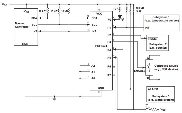
The PCF8574 I/O expander extends the usable pins in I2C LCD displays by leveraging its two main pins: SDA and SCL. This extension mechanism adds up to 8 additional pins labeled from P0 to P7. The LCD data pins—RS, RW, E, D4, D5, D6, and D7—are intricately connected to the corresponding pins on the PCF8574.
This configuration simplifies the design process and brings enhanced flexibility and scalability to projects requiring multiple I/O operations. You have found that carefully setting the address pins can avert conflicts, especially when multiple I2C devices coexist on a single bus. Such meticulous settings lend a tangible sense of relief, knowing that device compatibility and seamless operation are within reach.
PCF8574T Manufacturer
NXP Semiconductors N.V. is a well-regarded company in the field of semiconductor design and manufacturing. Its headquarters is located in Eindhoven, Netherlands. The firm employs about 29,000 people spread across more than 30 countries, marking a strong global footprint. Originally, NXP emerged as a spin-off from Philips in 2006. Then, in 2010, it transitioned to a publicly traded company with the ticker symbol NXPI. The company's stature and portfolio received a boost from its merger with Freescale Semiconductor in 2015.
In 2016, Qualcomm showed substantial interest in acquiring NXP. However, due to regulatory challenges, this acquisition attempt was ultimately abandoned in 2018. NXP's ability to navigate market expansions and regulatory landscapes while executing strategic mergers demonstrates its resilience and adaptability.
PCF8574T Block Diagram
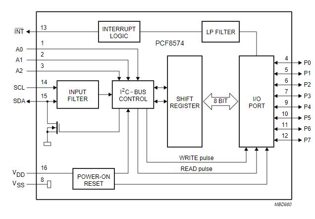
To gain an in-depth understanding of the PCF8574T I/O expander's internal structure and operation, refer to the typical block diagram. The PCF8574T serves as a versatile I/O expander, enhancing the I/O capabilities of microcontrollers across diverse applications. Think of industrial automation, home automation, and consumer electronics—these fields can all exploit its capabilities. Delving into the block diagram offers into how internal components work harmoniously to ensure seamless I/O expansion.
The input filter ensure signals received are devoid of noise and glitches. This filtering is essential for reliable I/O operation. Stabilizing inputs, it guarantees that only clean signals progress to the internal circuitry. Serving as the communication backbone, the I2C interface enables interaction between the PCF8574T and the host microcontroller. It meticulously handles the standard I2C protocol, ensuring a robust and efficient data transfer process, and enhancing the performance of the overall system. Control logic orchestrates the operational behavior of the PCF8574T. It deciphers commands from the I2C interface and manages data flow between the microcontroller and I/O pins. This component ensures that the expander accurately mirrors the intended states and operations as directed by the firmware. Understanding its internal architecture grants valuable into optimizing this I/O expander's use in varied applications.
Parts with Comparable Specifications
|
Part Number |
PCF8574T/3,512 |
PCF8574AT/3,518 |
PCF8574AT/3,512 |
PCF8574ADW |
PCA9554AD,112 |
|
Manufacturer |
NXP USA Inc. |
NXP USA Inc. |
NXP USA Inc. |
Texas Instruments |
NXP USA Inc. |
|
Package / Case |
16-SOIC (0.295, 7.50mm Width) |
16-SOIC (0.295, 7.50mm Width) |
16-SOIC (0.295, 7.50mm Width) |
16-SOIC (0.295, 7.50mm Width) |
16-SOIC (0.295, 7.50mm Width) |
|
Interface |
I2C |
I2C |
I2C, SMBus |
I2C |
I2C |
|
Supply Voltage |
5V |
5V |
3V |
5V |
5V |
|
Technology |
CMOS |
CMOS |
CMOS |
CMOS |
CMOS |
|
Terminal Pitch |
1.27mm |
1.27mm |
1.27mm |
1.27mm |
1.27mm |
|
Pin Count |
16 |
16 |
16 |
16 |
16 |
|
Width |
7.5mm |
7.5mm |
7.5mm |
7.5mm |
7.5mm |
|
Number of Ports |
1 |
1 |
1 |
1 |
1 |
Selecting an appropriate I/O expander from the listed options demands an in-depth understanding of the specific requirements and limitations of the intended application. Differences in voltage tolerance, thermal performance, and compatibility with complementary components can greatly affect the overall functionality and dependability of the design. These considerations can make an impact on both the efficiency and reliability of the final product.
 ABOUT US
Customer satisfaction every time. Mutual trust and common interests.
function test. The highest cost-effective products and the best service is our eternal commitment.
Hot Article
- Are CR2032 and CR2016 Interchangeable
- MOSFET: Definition, Working Principle and Selection
- Relay Installation and Testing, Interpretation of Relay Wiring Diagrams
- CR2016 vs. CR2032 What’s the difference
- NPN vs. PNP: What's the Difference?
- esp32 vs stm32: which microcontroller is better for you?
- LM358 Dual Operational Amplifier Comprehensive Guide: Pinouts, Circuit Diagrams, Equivalents, Useful Examples
- CR2032 VS DL2032 VS CR2025 Comparison Guide
- Understanding the Differences ESP32 and ESP32-S3 Technical and Performance Analysis
- Detailed Analysis of RC Series Circuit
 DHT11 vs DHT22: Detailed Pinout and Feature Comparison
2024-10-09
 TL072A JFET Dual Op-Amp
2024-10-08
Frequently Asked Questions [FAQ]
1. What is I2C converter?
I2C LCD adapter is a device containing a micro-controller PCF8574 chip.
2. What is I2c module?
I2C Module has an inbuilt PCF8574 I2C chip that converts I2C serial data to parallel data for the LCD display.
3. What is I2C used for?
The I2C protocol is used to establish communication between two or more ICs (Integrated Circuits), hence why it's known as Inter-Integrated Circuit (I2C) communication.
4. How do I program PCF8574?
After connecting the I2C Module to LCD, connect the GND and VCC pins of the PCF8574 Module to the GND and 5V pins of Arduino. Finally, the SDA and SCL Pins. Connect them to pins A4 and A5 pins of Arduino UNO respectively.
5. What is pcf8574t?
The PCF8574/74A provides general-purpose remote I/O expansion via the two-wire bidirectional I2C-bus (serial clock (SCL), serial data (SDA)). The devices consist of eight quasi-bidirectional ports, a 100 kHz I2C-bus interface, three hardware address inputs, and interrupt output operating between 2.5 V and 6 V.
Hot Part Number
 C1608CH2E102J080AA
 GQM2195C1H300JB01D
 GRM0337U1E560JD01D
 GCM0335C1E8R3DD03D
 C1608JB0J335M080AB
 CY7C1347F-133AC
 EPF8452AQC160-2
 AT49F1025-70VC
 SY88803VKC
 6MBI300U-120A-05
- ADS7250IRTET
- XCR3128XL-10TQ144I
- SN74LVC1G125DBVT
- TPS2010APWP
- DM870-TE
- CS8182YDFR8G
- MM74HC32MTC
- SIR638ADP-T1-RE3
- CD4011BCM
- DMP2045U-7
- LPV358IDDURE4
- ADUM2200BRWZ-RL
- LT3971AIMSE-5#PBF
- AT45DB161B-TU
- CAT522W-TE13
- CMP100N03
- CY2292FZ
- MB91F233LALGV-G
- MK1493-03BGTR
- NJM2564A
- SM2246EN
- STI5197-CBB
- USB2601-NU-06
- VCA8617PAGRR
- AR5312A-001
- GS8162Z36BD-200
- IC42S16400-6T
- KE44B-25AN/2GB
- U2044B-MFPG3Y
- MT47H64M16M16HR-3:H
- TMSC138G052PZ
- BH76095GU-E2
- MN101C54CMT
- MN15G1601XE1
- CXP82032-152Q
- AP6690S
- TBD62308AFAGEL
- SKY85784-11
- DTS-61N-V